- Collections
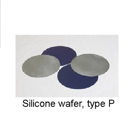
Silicon wafer, type P
These silicon wafers can be used for substrate studies or as substrate for AFM and SEM samples by cleaving the wafer.Specifications1 in2 in3 in4 in6 inMaterial:SiliconSiliconSiliconSiliconSiliconDiameter:25 mm50 mm76 mm100 mm150 mmOrientation:<100><100><111><100><100>Resistance:1-30 Ohms1-30 Ohms1-30 Ohms1-30 Ohms1-30 OhmsType P:Boron - 1 primary flatBoron - 1 primary flatBoron - 1 primary flatBoron - 1 primary flatBoron - 1 primary flatSiO2 top coating:NoneNone...
These silicon wafers can be used for substrate studies or as substrate for AFM and SEM samples by cleaving the wafer.
Specifications
| 1 in | 2 in | 3 in | 4 in | 6 in | |
| Material: | Silicon | Silicon | Silicon | Silicon | Silicon |
| Diameter: | 25 mm | 50 mm | 76 mm | 100 mm | 150 mm |
| Orientation: | <100> | <100> | <111> | <100> | <100> |
| Resistance: | 1-30 Ohms | 1-30 Ohms | 1-30 Ohms | 1-30 Ohms | 1-30 Ohms |
| Type P: | Boron - 1 primary flat | Boron - 1 primary flat | Boron - 1 primary flat | Boron - 1 primary flat | Boron - 1 primary flat |
| SiO2 top coating: | None | None | None | None | None |
| Wafer Thickness: | 10-12 mill (254-304µm) |
9-13 mill (230-330µm) |
13.6-18.5 mill (345-470µm) |
18.7-22.6 mill (475-575µm) |
23.6-25.2 mill (600-690µm) |
| Roughness: | 2nm | 2nm | 2nm | 2nm | 2nm |
| TTV: | <20µm | ||||
| Polished: | on one side | on one side | on one side | on one side | on one side |
Please choose carefully. Returns of this item are subject to approval.
| Code | Title | Size | Pack Size | Availability | Price | Updated: 11-05-2024 |
|---|---|---|---|---|---|---|
| EMS71893-04 | Silicon wafer, type P | 1 inch | Each | See above | $93.00 AUD | |
| EMS71893-05 | Silicon wafer, type P | 2 inch | Each | See above | $61.00 AUD | |
| EMS71893-06 | Silicon wafer, type P | 3 inch | Each | See above | $63.00 AUD | |
| EMS71893-07 | Silicon wafer, type P | 4 inch | Each | 1 in stock | $91.00 AUD | |
| EMS71893-08 | Silicon wafer, type P | 6 inch | Each | See above | $124.00 AUD | |